LIVA: LIthographic Variation Aware timing analyzer
Project Director: David Z. Pan
Student: Yongchan Ban
Introduction
Even with technology scaling below 45nm, the lithography tools have remained at 193nm
resulting in significant variations. These variations impact the performance, yield and reliability
of the designs. There are two types of lithography variations introduced that result in such nonrectangular
gate dimensions: systematic lithography variations and random variations. In order to
analyze and overcome these variations, we report an accurate extraction toolkit for model-based
geometrical and electrical analysis that accounts for both systematic lithography variations, e.g.,
gate poly contours and diffusion rounding, and random lithography variation, e.g., line-edgeroughness
(LER) and contact-edge-roughness (CER). For the non-rectangular gate extraction, we
use a gate segmentation approach in which the basic idea is to convert a non-rectangular
transistor into several rectangular slices such that the non-rectangular gate shape is modeled as a
single equivalent rectangular transistor with an effective gate length. We also account for gate
LER and contact CER, and model it with the systematic contour-based variations in a single
characterization flow.
Software
LIVA 1.0
Author: Yongchan Ban. Copyright (c) The University of Texas, 2009. All rights reserved.
IF YOU AGREE TO THE UT RESEARCH LICENSE, PLEASE FILL IN FOLLOWING FORM. THE CODE WILL BE DISTRIBUTED TO YOU ONCE YOU ARE APPROVED.
Publication
- Yongchan Ban and David Z. Pan, "Compact Modeling and Robust Layout Optimization for Contacts in Deep Subwavelength Lithography", ACM/IEEE Design Automation Conference (DAC), June 2010.
- Yongchan Ban, Savithri Sundareswaran, and David Z. Pan, "Total Sensitivity Based DFM Optimization of Standard Library Cells", International Symposium on Physical Design (ISPD), March 2010.
- Yongchan Ban, Yuansheng Ma, Harry J. Levinson, Yunfei Deng, Jongwook Kye, and David Z. Pan, " Modeling and Characterization of Contact Edge Roughness for Minimizing Design and Manufacturing Variations in 32-nm Node Standard Cell ", Intl. Symp. SPIE Advanced Lithography, February 2010.
- Yongchan Ban, Savithri Sundareswaran, and David Z. Pan, "Comprehensive Standard Cell Characterization Considering Random Line-Edge Roughness Lithography Variation", SRC Techcon Conference, Austin, TX, September 2009.
- Yong-Chan Ban, David Z. Pan, Savithri Sundareswaran and Rajendran Panda, "Electrical Impact of Line-Edge Roughness on Sub-45nm Node Standard Cell", Intl.Symp. SPIE Advanced Lithography, February 2009.
Overall Flow
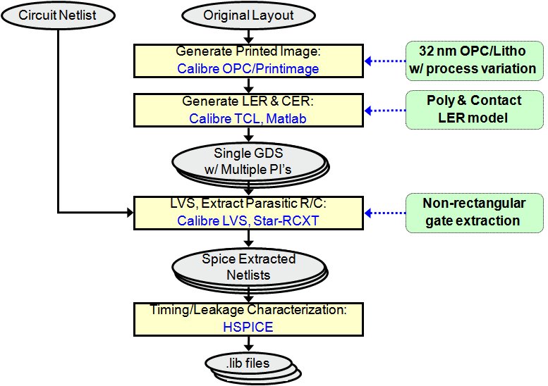
Above Figure illustrates the overall flow of our model-based geometrical
and electrical analysis toolkit. The flow is divided into three main steps:
- Print Image Simulation: this step involves simulating the
lithography models and generation of non-rectangular contours/shapes due to the
printed image. We use a commercial OPC and lithography simulation tools to get the
print-images of the nominal condition and the process corners. After done
lithography print-image simulation, rule-based etch corrections for etch
proximity effects are applied to the print-images. Once we get the final print-images,
we can also simulate the impact of LER and CER. Input LER conditions are first
requested, and then the LER and CER variations are added on the edge of the
final print-images. Thus, there need an OPC/print-image runset file, an optical
model file, a photoresist setup file, etch rules and LER/CER input conditions.
- Extraction with print-image: this step extracts device
dimensions considering the non-rectangular shape in the poly and diffusion
layers due to print image. To get the parasitic resistance and capacitance
parameters of a cell, we use a commercial layout extraction tool, meanwhile we
back-annotate the more detail information of active devices by the
non-rectangular transistor extraction model. The basic idea is to convert a
non-rectangular transistor into several slices such that the non-rectangular
gate shape is modeled as a single equivalent rectangular transistor with an
effective gate length. An original circuit netlist file, a LVS runset and model
files and a layout extraction runset and model files are input in this step.
- Delay and Power Characterization: this step characterizes the
cells for delay and leakage information using the extracted parameters from
previous step. We use a commercial circuit simulation tool to get delay and power
of a cell for each process corners. A spice netlist and model files are
required in this step.
The simulated print-image is
written to a new layout file, which is an input file for an extraction tool. We
use an industrial extraction tool to extract the devices and the parasitic in a
spice netlist format. This extraction is then updated with actual gate length
values, followed by timing and power analysis with an industrial circuit simulator.
All the sequences are implemented and automated in our cell characterization
flow.
last updated by January 28 2010